The account of this former contributor was not re-activated after the server upgrade of March 2022.
Circuits
Miscellaneous
| Miscellaneous
|
|
|
(PD) Diagram: John R. Brews
|
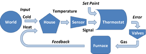
Thermostatic control of house temperature
|
|
|
(PD) Diagram: John R. Brews
|
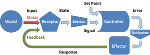
Negative feedback as a model for homeostasis
|
|
|
(PD) Diagram: John R. Brews
|
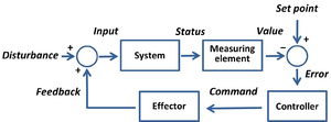
Feedback control to set system status at a set point
|
|
|
(PD) Diagram: John R. Brews
|
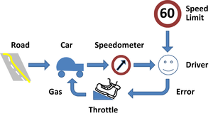
Keeping a car at the speed limit using negative feedback
|
|
Current sources
| Current sources
|
|
|
(CC) Image: John R. Brews
|
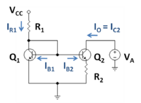
Widlar current source using bipolar transistors
|
|
|
(CC) Image: John R. Brews
|
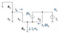
Small-signal circuit for finding output resistance of the Widlar source
|
|
|
(CC) Image: John R. Brews
|
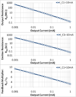
Design trade-off between output resistance and output current in Widlar source
|
|
|
(PD) Image: John R. Brews
|
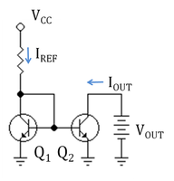
A current mirror implemented with npn bipolar transistors using a resistor to set the reference current IREF; VCC = supply voltage.
|
|
|
(PD) Image: John R. Brews
|
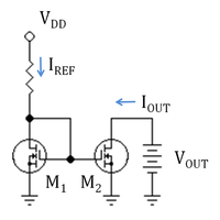
An n-channel MOSFET current mirror with a resistor to set the reference current
|
|
|
(PD) Image: John R. Brews
|
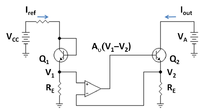
Gain-boosted current mirror with op amp feedback to increase output resistance.
|
|
|
(PD) Image: John R. Brews
|
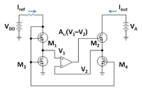
MOSFET version of wide-swing current mirror; M1 and M2 are in active mode
|
|
|
(PD) Image: John R. Brews
|
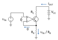
Operational-amplifier based current sink. Because the op amp is modeled as a nullor, op amp input variables are zero regardless of the values for its output variables.
|
|
|
(PD) Image: John R. Brews
|
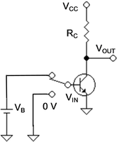
A digital inverter circuit using a bipolar transistor.
|
|
|
(PD) Image: John R. Brews
|
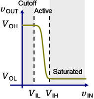
Transfer characteristic of bipolar inverter showing modes.
|
|
|
|
|
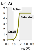
Collector current vs. input voltage for a bipolar inverter with VCC=5V and RC=1kΩ.
|
|
|
(PD) Image: John R. Brews
|
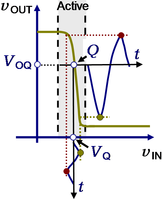
Input and output signals for bipolar inverter used as an amplifier.
|
|
|
(PD) Image: John R. Brews
|
Two-port network with symbol definitions.
|
|
|
(PD) Image: John R. Brews
|
Z-equivalent two port showing independent variables I1 and I2.
|
|
|
(PD) Image: John R. Brews
|
Y-equivalent two port showing independent variables
|
|
|
(PD) Image: John R. Brews
|
H-equivalent two-port showing independent variables
|
|
|
(PD) Image: John R. Brews
|
G-equivalent two-port showing independent variables
|
|
|
(PD) Image: John R. Brews
|
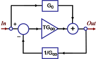
Block diagram for asymptotic gain model
|
|
|
(PD) Image: John R. Brews
|
Possible signal-flow graph for the asymptotic gain model
|
|
|
(PD) Image: John R. Brews
|
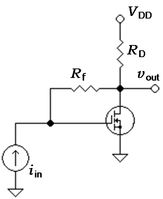
MOSFET transresistance feedback amplifier.
|
|
|
(PD) Image: John R. Brews
|
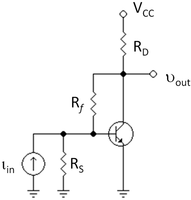
Collector-to-base biased bipolar amplifier.
|
|
|
(PD) Image: John R. Brews
|
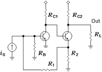
Two-transistor feedback amplifier; any source impedance RS is lumped in with the base resistor RB.
|
|
Small-signal circuits
| Small-signal circuits
|
|
|
(PD) Image: John R. Brews
|
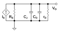
Small-signal circuit for pn-diode driven by a current signal represented as a Norton source.
|
|
|
(PD) Image: John R. Brews
|
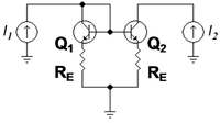
Bipolar current mirror with emitter resistors
|
|
|
(PD) Image: John R. Brews
|
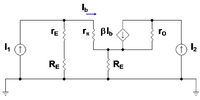
Small-signal circuit for bipolar current mirror
|
|
|
(PD) Image: John R. Brews
|
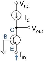
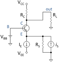
Common base circuit with active load and current drive.
|
|
|
(PD) Image: John R. Brews
|
Common-base amplifier with AC current source I1 as signal input
|
|
|
(PD) Image: John R. Brews
|
Bipolar transistor with base grounded and signal applied to emitter.
|
|
|
(PD) Image: John R. Brews
|
Common-base amplifier with AC voltage source V1 as signal input
|
|
|
(PD) Image: John R. Brews
|
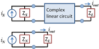
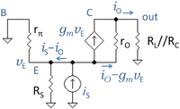
The result of applying Norton's theorem.
|
|
|
(PD) Image: John R. Brews
|
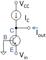
Bipolar current buffer.
|
|
|
(PD) Image: John R. Brews
|
Small-signal circuit to find output current.
|
|
|
(PD) Image: John R. Brews
|
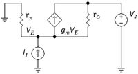
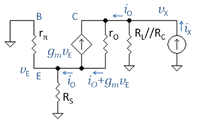
Small-signal circuit with test current iX to find Norton resistance.
|
|
|
(PD) Image: John R. Brews
|
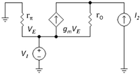
The result of applying Thévenin's theorem.
|
|
|
(PD) Image: John R. Brews
|
Bipolar buffer.
|
|
|
(PD) Image: John R, Brews
|
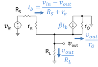
Small-signal circuit for voltage follower.
|
|
|
(PD) Image: John R. Brews
|
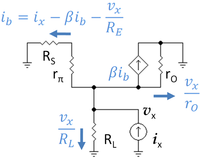
Determination of the small-signal output resistance.
|
|
|
(PD) Image: John R. Brews
|
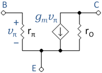
Simplified, low-frequency hybrid-pi BJT model.
|
|
|
(PD) Image: John R. Brews
|
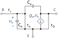
Bipolar hybrid-pi model with parasitic capacitances.
|
|
|
(PD) Image: John R. Brews
|
Simplified, low-frequency hybrid-pi BJT model.
|
|
|
(PD) Image: John R. Brews
|
Bipolar hybrid-pi model with parasitic capacitances.
|
|
|
(PD) Image: John R. Brews
|
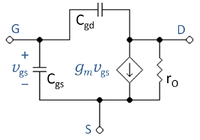
Simplified, three-terminal MOSFET hybrid-pi model.
|
|
|
(PD) Image: John R. Brews
|
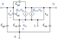
Four-terminal small-signal MOSFET circuit.
|
|
|
(PD) Image: John R. Brews
|
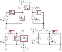
Miller effect: These two circuits are equivalent.
|
|
|
(PD) Image: John R. Brews
|
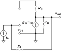
Small-signal circuit for transresistance amplifier
|
|
|
(PD) Image: John R. Brews
|
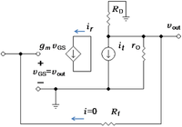
Small-signal circuit with return path broken and test current it driving amplifier at the break.
|
|
|
(PD) Image: John R. Brews
|
Three small-signal schematics used to discuss the asymptotic gain model
|
|
Return ratio
| Return ratio
|
|
|
(PD) Image: John R. Brews
|
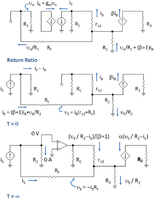
Left - small-signal circuit corresponding to bipolar amplifier; Center - inserting independent source and marking leads to be cut; Right - cutting the dependent source free and short-circuiting broken leads.
|
|
Amplifiers
| Amplifiers
|
|
|
(PD) Image: John R. Brews
|
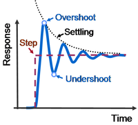
Some terms used to describe step response in time domain.
|
|
|
(PD) Image: John R. Brews
|
Ideal negative feedback model; open loop gain is AOL and feedback factor is β.
|
|
|
(PD) Image: John R. Brews
|
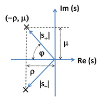
Conjugate pole locations for step response of two-pole feedback amplifier.
|
|
|
(PD) Image: John R. Brews
|
Step-response of a linear two-pole feedback amplifier.
|
|
|
(PD) Image: John R. Brews
|
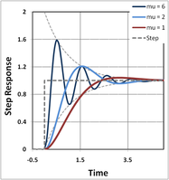
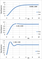
Step response for three values of time constant ratio.
|
|
|
(PD) Image: John R. Brews
|
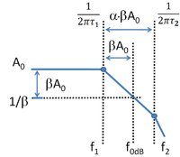
Bode gain plot to find phase margin of two-pole amplifier.
|
|
|
(PD) Image: John R. Brews
|
|
|
|
|
(PD) Image: John R. Brews
|
|
|
|
|
(PD) Image: John R. Brews
|
Bode magnitude plot for zero and for low-pass pole
|
|
|
(PD) Image: John R. Brews
|
Bode phase plot for zero and for low-pass pole
|
|
|
(PD) Image: John R. Brews
|
Bode magnitude plot for pole-zero combination; the location of the zero is ten times higher than in above figures
|
|
|
(PD) Image: John R. Brews
|
Bode phase plot for pole-zero combination; the location of the zero is ten times higher than in above figures
|
|
|
(PD) Image: John R. Brews
|
Gain of feedback amplifier AFB in dB and corresponding open-loop amplifier AOL.
|
|
|
(PD) Image: John R. Brews
|
Phase of feedback amplifier °AFB in degrees and corresponding open-loop amplifier °AOL.
|
|
|
(PD) Image: John R. Brews
|
Gain of feedback amplifier AFB in dB and corresponding open-loop amplifier AOL.
|
|
|
(PD) Image: John R. Brews
|
Phase of feedback amplifier AFB in degrees and corresponding open-loop amplifier AOL.
|
|
|
(PD) Image: John R. Brews
|
Operational amplifier with compensation capacitor CC between input and output to cause pole splitting.
|
|
|
(PD) Image: John R. Brews
|
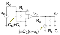
Operational amplifier with compensation capacitor transformed using Miller's theorem to replace the compensation capacitor with a Miller capacitor at the input and a frequency-dependent current source at the output.
|
|
|
(PD) Image: John R. Brews
|
Idealized Bode plot for a two pole amplifier design.
|
|
|
(PD) Image: John R. Brews
|
Miller capacitance at low frequencies CM (top) and compensation capacitor CC (bottom) as a function of gain
|
|
