User:John R. Brews/WP Import
The hybrid-pi model is a popular circuit model used for analyzing the small signal behavior of transistors. The model can be quite accurate for low-frequency circuits and can easily be adapted for higher frequency circuits with the addition of appropriate inter-electrode capacitances and other parasitic elements.
Bipolar transistor
The hybrid-pi model is a linearized two-port network approximation to the transistor using the small-signal base-emitter voltage and collector-emitter voltage as independent variables, and the small-signal base current and collector current as dependent variables. (See Jaeger and Blalock.[1])
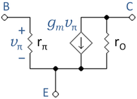
A basic, low-frequency hybrid-pi model for the bipolar transistor is shown in the figure. The three transistor terminals are E = emitter, B = base, and C = collector. The base-emitter connection is through a resistor rπ, and the base current causes a small-signal voltage drop across it, vπ (the π notation is standard). The various parameters are as follows.
- is the transconductance in siemens, evaluated in a simple model (see Jaeger and Blalock[2])
- where:
- is the quiescent collector current (also called the collector bias or DC collector current)
- is the thermal voltage, calculated from Boltzmann's constant, the charge on an electron, and the transistor temperature in kelvins. At 290 K VT is very nearly 25 mV (Google calculator)(room temperature or 70°F ≈ 294 K).
- in ohms
- where:
- is the current gain at low frequencies (commonly called hFE). Here is the Q-point base current. This is a parameter specific to each transistor, and can be found on a datasheet; is a function of the choice of collector current.
- is the output resistance due to the Early effect.
Related terms
The reciprocal of the output resistance is named the output conductance
- .
The reciprocal of gm is called the intrinsic resistance
- .
MOSFET parameters

A basic, low-frequency hybrid-pi model for the MOSFET is shown in figure 2. The various parameters are as follows.
is the transconductance in siemens, evaluated in the Shichman-Hodges model in terms of the Q-point drain current by (see Jaeger and Blalock[3]):
- ,
- where:
- is the quiescent drain current (also called the drain bias or DC drain current)
- = threshold voltage and = gate-to-source voltage.
The combination:
often is called the overdrive voltage.
- is the output resistance due to channel length modulation, calculated using the Shichman-Hodges model as
- ,
using the approximation for the channel length modulation parameter λ[4]
- .
Here VE is a technology related parameter (about 4 V / μm for the 65 nm technology node[4]) and L is the length of the source-to-drain separation.
The reciprocal of the output resistance is named the drain conductance
- .
References and notes
- ↑ R.C. Jaeger and T.N. Blalock (2004). Microelectronic Circuit Design, Second Edition. New York: McGraw-Hill, Section 13.5, esp. Eqs. 13.19. ISBN 0-07-232099-0.
- ↑ R.C. Jaeger and T.N. Blalock. Eq. 5.45 pp. 242 and Eq. 13.25 p. 682. ISBN 0-07-232099-0.
- ↑ R.C. Jaeger and T.N. Blalock. Eq. 4.20 pp. 155 and Eq. 13.74 p. 702. ISBN 0-07-232099-0.
- ↑ 4.0 4.1 W. M. C. Sansen (2006). Analog Design Essentials. Dordrechtμ: Springer. ISBN 0-387-25746-2.


