User:John R. Brews/WP Import: Difference between revisions
imported>John R. Brews No edit summary |
imported>John R. Brews |
||
| Line 17: | Line 17: | ||
== Impedance parameters (z-parameters)== | == Impedance parameters (z-parameters)== | ||
{{Image|Z-equivalent two-port.PNG|right|350px| z-equivalent two port showing independent variables ''I<sub>1</sub>'' and ''I<sub>2</sub>''.}} | |||
The figure shows the two-port driven by two external current sources, making the input currents ''I<sub>1</sub>'' and ''I<sub>2</sub>'' the independent variables controlled from outside the two-port. The port voltages are determined in terms of these input currents by the ''z''-parameters defined by: | |||
:<math> \left[ \begin{array}{c} V_1 \\ V_2 \end{array} \right] = \left[ \begin{array}{cc} z_{11} & z_{12} \\ z_{21} & z_{22} \end{array} \right] \left[ \begin{array}{c}I_1 \\ I_2 \end{array} \right] </math>. | :<math> \left[ \begin{array}{c} V_1 \\ V_2 \end{array} \right] = \left[ \begin{array}{cc} z_{11} & z_{12} \\ z_{21} & z_{22} \end{array} \right] \left[ \begin{array}{c}I_1 \\ I_2 \end{array} \right] </math>. | ||
Revision as of 12:03, 20 May 2011

Two-port network with symbol definitions. A Thevenin voltage source with Thevenin impedance ZTh drives port 1, and impedance ZL loads port 2
A two-port network is an electrical circuit with two pairs of terminals. As shown in the figure, two terminals constitute a port only if they satisfy the essential requirement known as the port condition, namely, the same current must enter and leave a port.[1][2] Examples include small-signal models for transistors (such as the hybrid-pi model), filters and matching networks. The analysis of passive two-port networks is an outgrowth of reciprocity theorems first derived by Lorentz.[3]
A two-port network makes possible the replacement of either a complete circuit or part of it by a "black box" with a only four distinct parameters, enabling us to separate its behavior from that of its internal constituents, thus simplifying analysis. Any linear circuit with four terminals can be transformed into a two-port network provided that it does not contain an independent source and satisfies the port conditions.
The parameters used in order to describe a two-port network are the following: z, y, h, g, T. They are usually expressed in matrix notation and they establish relations between the port currents and voltages (see the figure):
- = Port 1 voltage
- = Port 1 current
- = Port 2 voltage
- = Port 2 current
These variables are most useful at low to moderate frequencies. At high frequencies (for example, microwave frequencies) power and energy are more useful variables, and the two-port approach based on current and voltages that is discussed here is replaced by an approach based upon scattering parameters.
Though some authors use the terms two-port network and four-terminal network interchangeably, the latter represents a more general concept. Not all four-terminal networks are two-port networks. A pair of terminals can be called a port only if the current entering one is equal to the current leaving the other (the port condition). Only those four-terminal networks in which the four terminals can be paired into two ports can be called two-ports.[1][2]
Impedance parameters (z-parameters)
The figure shows the two-port driven by two external current sources, making the input currents I1 and I2 the independent variables controlled from outside the two-port. The port voltages are determined in terms of these input currents by the z-parameters defined by:
- .
Notice that all the z-parameters have dimensions of ohms.
Example: bipolar current mirror with emitter degeneration
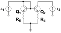
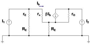
Figure 3 shows a bipolar current mirror with emitter resistors to increase its output resistance.[4] Transistor Q1 is diode connected, which is to say its collector-base voltage is zero. Figure 4 shows the small-signal circuit equivalent to Figure 3. Transistor Q1 is represented by its emitter resistance rE ≈ VT / IE (VT = thermal voltage, IE = Q-point emitter current), a simplification made possible because the dependent current source in the hybrid-pi model for Q1 draws the same current as a resistor 1 / gm connected across rπ. The second transistor Q2 is represented by its hybrid-pi model. Table 1 below shows the z-parameter expressions that make the z-equivalent circuit of Figure 2 electrically equivalent to the small-signal circuit of Figure 4.
| Table 1 | Expression | Approximation |
|---|---|---|
The negative feedback introduced by resistors RE can be seen in these parameters. For example, when used as an active load in a differential amplifier, I1 ≈ -I2, making the output impedance of the mirror approximately R22 -R21 ≈ 2 β rORE /( rπ+2RE ) compared to only rO without feedback (that is with RE = 0 Ω) . At the same time, the impedance on the reference side of the mirror is approximately R11 -R12 ≈ , only a moderate value, but still larger than rE with no feedback. In the differential amplifier application, a large output resistance increases the difference-mode gain, a good thing, and a small mirror input resistance is desirable to avoid Miller effect.
Admittance parameters (y-parameters)
- .
where
The network is said to be reciprocal if . Notice that all the Y-parameters have dimensions of siemens.
Hybrid parameters (h-parameters)
- .
where
Often this circuit is selected when a current amplifier is wanted at the output. The resistors shown in the diagram can be general impedances instead.
Notice that off-diagonal h-parameters are dimensionless, while diagonal members have dimensions the reciprocal of one another.
Example: common base amplifier
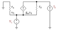
Note: Tabulated formulas in Table 2 make the h-equivalent circuit of the transistor from Figure 6 agree with its small-signal low-frequency hybrid-pi model in Figure 7. Notation: rπ = base resistance of transistor, rO = output resistance, and gm = transconductance. The negative sign for h21 reflects the convention that I1, I2 are positive when directed into the two-port. A non-zero value for h12 means the output voltage affects the input voltage, that is, this amplifier is bilateral. If h12 = 0, the amplifier is unilateral.
| Table 2 | Expression | Approximation |
|---|---|---|
| << 1 |
Inverse hybrid parameters (g-parameters)
- .
where
Often this circuit is selected when a voltage amplifier is wanted at the output. Notice that off-diagonal g-parameters are dimensionless, while diagonal members have dimensions the reciprocal of one another. The resistors shown in the diagram can be general impedances instead.
Example: common base amplifier
Note: Tabulated formulas in Table 3 make the g-equivalent circuit of the transistor from Figure 8 agree with its small-signal low-frequency hybrid-pi model in Figure 9. Notation: rπ = base resistance of transistor, rO = output resistance, and gm = transconductance. The negative sign for g12 reflects the convention that I1, I2 are positive when directed into the two-port. A non-zero value for g12 means the output current affects the input current, that is, this amplifier is bilateral. If g12 = 0, the amplifier is unilateral.
| Table 3 | Expression |
|---|---|
ABCD-parameters
The ABCD-parameters are known variously as chain, cascade, or transmission parameters.[5]
- .
where
Note that we have inserted negative signs in front of the fractions in the definitions of parameters B and D. The reason for adpoting this convention (as opposed to the convention adopted above for the other sets of parameters) is that it allows us to represent the transmission matrix of cascades of two or more two-port networks as simple matrix multiplications of the matrices of the individual networks. This convention is equivalent to reversing the direction of I2 so that it points in the same direction as the input current to the next stage in the cascaded network.
This technique is exactly analogous to the use of ABCD matrices for ray tracing in the science of optics. See also ray transfer matrix.
Table of transmission parameters
The table below lists transmission parameters for some simple network elements.
| Element | Matrix | Remarks |
|---|---|---|
| Series resistor | R = resistance | |
| Shunt resistor | R = resistance | |
| Series conductor | G = conductance | |
| Shunt conductor | G = conductance | |
| Series inductor | L = inductance s = complex angular frequency | |
| Shunt capacitor | C = capacitance s = complex angular frequency |
Combinations of two-port networks
Series connection of two 2-port networks: Z = Z1 + Z2
Parallel connection of two 2-port networks: Y = Y1 + Y2
Example: Cascading two networks
Suppose we have a two-port network consisting of a series resistor R followed by a shunt capacitor C. We can model the entire network as a cascade of two simpler networks:
The transmission matrix for the entire network T is simply the matrix multiplication of the transmission matrices for the two network elements:
Thus:
Notes regarding definition of transmission parameters
1) It should be noted that all these examples are specific to the definition of transmission parameters given here. Other definitions exist in the literature, such as:
2) The format used above for cascading (ABCD) examples cause the "components" to be used backwards compared to standard electronics schematic conventions. This can be fixed by taking the transpose of the above formulas, or by making the the left hand side (dependent variables). Another advantage of the form is that the output can be terminated (via a transfer matrix representation of the load) and then can be set to zero; allowing the voltage transfer function, 1/A to be read directly.
3) In all cases the ABCD matrix terms and current definitions should allow cascading. 4
Networks with more than 2 ports
While two port networks are very common (e.g. amplifiers and filters), other electrical networks such as directional couplers and isolators have more than 2 ports. The following representations can be extended to networks with an arbitrary number of ports:
They are extended by adding appropriate terms to the matrix representing the other ports. So 3 port impedance parameters result in the following relationship:
- .
It should be noted that the following representations cannot be extended to more than two ports:
- Hybrid (h) parameters
- Inverse hybrid (g) parameters
- Transmission (ABCD) parameters
- Scattering Transmission (T) parameters
References
- ↑ 1.0 1.1 P.R. Gray, P.J. Hurst, S.H. Lewis, and R.G. Meyer (2001). Analysis and Design of Analog Integrated Circuits, Fourth Edition. New York: Wiley, §3.2, p. 172. ISBN 0471321680.
- ↑ 2.0 2.1 R. C. Jaeger and T. N. Blalock (2006). Microelectronic Circuit Design, Third Edition. Boston: McGraw-Hill, §10.5 §13.5 §13.8. ISBN 9780073191638.
- ↑ See review by Jasper J. Goedbloed (2003). Reciprocity and EMC measurements. Presentation at 2003 EMC Zurich Symposium and as IEEE EMC EMCS Newsletter pp.93-104.
- ↑ The emitter-leg resistors counteract any current increase by decreasing the transistor VBE. That is, the resistors RE cause negative feedback that opposes change in current. In particular, any change in output voltage results in less change in current than without this feedback, which means the output resistance of the mirror has increased.
- ↑ David M. Pozar (2005). Microwave Engineering, 3rd Edition. John Wiley & Sons, Chapter 4: pp. 161-221. ISBN 047164451X (Softcover).


![{\displaystyle \left[{\begin{array}{c}V_{1}\\V_{2}\end{array}}\right]=\left[{\begin{array}{cc}z_{11}&z_{12}\\z_{21}&z_{22}\end{array}}\right]\left[{\begin{array}{c}I_{1}\\I_{2}\end{array}}\right]}](https://wikimedia.org/api/rest_v1/media/math/render/svg/7645f82f97b057892f6d77d80bbf01b985aaae0f)


![{\displaystyle \left[{\begin{array}{c}I_{1}\\I_{2}\end{array}}\right]=\left[{\begin{array}{cc}y_{11}&y_{12}\\y_{21}&y_{22}\end{array}}\right]\left[{\begin{array}{c}V_{1}\\V_{2}\end{array}}\right]}](https://wikimedia.org/api/rest_v1/media/math/render/svg/1f0a34623af2771a0510c92e6a21ac4e6de760aa)


![{\displaystyle \left[{\begin{array}{c}V_{1}\\V_{2}\\V_{3}\end{array}}\right]=\left[{\begin{array}{ccc}Z_{11}&Z_{12}&Z_{13}\\Z_{21}&Z_{22}&Z_{23}\\Z_{31}&Z_{32}&Z_{33}\end{array}}\right]\left[{\begin{array}{c}I_{1}\\I_{2}\\I_{3}\end{array}}\right]}](https://wikimedia.org/api/rest_v1/media/math/render/svg/6f8103856d09b829a923cf5cf08e6269aae1139a)