User:John R. Brews/Circuits: Difference between revisions

From Citizendium
Jump to navigation Jump to search
imported>John R. Brews
(Created page with "==Circuits== {{Gallery-mixed |caption=Current sources |width=200 |lines=5 |Widlar Current Source.PNG|Widlar current source using bipolar transistors |Widlar small-signal.PNG|Smal...")
 
No edit summary
 
(6 intermediate revisions by one other user not shown)
Line 1: Line 1:
{{AccountNotLive}}
==Circuits==
==Circuits==
{{TOC|right}}
===Miscellaneous===
{{Gallery-mixed
|caption=Miscellaneous
|width=300
|lines=5
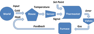
|Thermostat system.png|Thermostatic control of house temperature
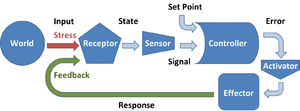
|Homeostasis.png|Negative feedback as a model for homeostasis
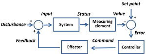
|Set-point control.png|Feedback control to set system status at a set point
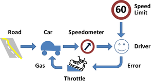
|Car feedback.png|Keeping a car at the speed limit using negative feedback
}}
===Current sources===
{{Gallery-mixed
{{Gallery-mixed
|caption=Current sources
|caption=Current sources
Line 27: Line 41:
|Shunt-series feedback amplifier.PNG|Two-transistor feedback amplifier; any source impedance ''R<sub>S</sub>'' is lumped in with the base resistor ''R<sub>B</sub>''.
|Shunt-series feedback amplifier.PNG|Two-transistor feedback amplifier; any source impedance ''R<sub>S</sub>'' is lumped in with the base resistor ''R<sub>B</sub>''.
}}
}}
===Small-signal circuits===
{{Gallery-mixed
{{Gallery-mixed
|caption=Small-signal circuits
|caption=Small-signal circuits
Line 56: Line 71:
|Return ratio.PNG|Small-signal circuit with return path broken and test current ''i<sub>t</sub>'' driving amplifier at the break.
|Return ratio.PNG|Small-signal circuit with return path broken and test current ''i<sub>t</sub>'' driving amplifier at the break.
|Using return ratio.PNG|Three small-signal schematics used to discuss the asymptotic gain model
|Using return ratio.PNG|Three small-signal schematics used to discuss the asymptotic gain model
}}
===Return ratio===
{{Gallery-mixed
|caption=Return ratio
|width=500
|lines=5
|Inserting source for return ratio.PNG|''Left'' - small-signal circuit corresponding to bipolar amplifier; ''Center'' - inserting independent source and marking leads to be cut; ''Right''  - cutting the dependent source free and short-circuiting broken leads.
}}
===Amplifiers===
{{Gallery-mixed
|caption=Amplifiers
|width=200
|lines=5
|Aspects of step response.PNG|Some terms used to describe step response in time domain.
|Negative feedback amplifier.PNG|Ideal negative feedback model; open loop gain is ''A''<sub>OL</sub> and feedback factor is β.
|Conjugate poles.PNG|Conjugate pole locations for step response of two-pole feedback amplifier.
|Step response of negative feedback amplifier.PNG| Step-response of a linear two-pole feedback amplifier.
|Overshoot control.PNG|Step response for three values of time constant ratio.
|Gain Bode plot for two-pole amplifier.PNG|Bode gain plot to find phase margin of two-pole amplifier.
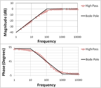
|High-pass amplifier Bode plot.PNG|The Bode plot for a first-order (one-pole) [[highpass filter]]
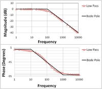
|Low-pass amplifier Bode plot.PNG|The Bode plot for a first-order (one-pole) [[lowpass filter]]
|Bode plot for pole and zero.PNG| Bode magnitude plot for zero and for low-pass pole
|Bode phase plot for pole and zero.PNG|Bode phase plot for zero and for low-pass pole
|Superposed Bode plots for pole and zero.PNG|Bode magnitude plot for pole-zero combination; the location of the zero is ten times higher than in above figures
|Superposed Bode phase plots for pole and zero.PNG|Bode phase plot for pole-zero combination; the location of the zero is ten times higher than in above figures
|Open and closed loop gain.PNG|Gain of feedback amplifier ''A''<sub>FB</sub> in dB and corresponding open-loop amplifier ''A''<sub>OL</sub>.
|Open and closed loop phase.PNG|Phase of feedback amplifier ''°A''<sub>FB</sub> in degrees and corresponding open-loop amplifier ''°A''<sub>OL</sub>.
|Gain margin.PNG|Gain of feedback amplifier ''A''<sub>FB</sub> in dB and corresponding open-loop amplifier ''A''<sub>OL</sub>.
|Phase margin.PNG|Phase of feedback amplifier ''A''<sub>FB</sub> in degrees and corresponding open-loop amplifier ''A''<sub>OL</sub>.
|Pole splitting example.PNG| Operational amplifier with compensation capacitor ''C<sub>C</sub>'' between input and output to cause pole splitting.
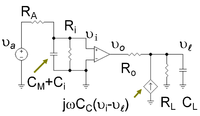
|Pole splitting with Miller transformation.PNG|Operational amplifier with compensation capacitor transformed using [[Miller effect|Miller's theorem]] to replace the compensation capacitor with a Miller capacitor at the input and a frequency-dependent current source at the output.
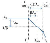
|Two-pole Bode magnitude plot.PNG|Idealized [[Bode plot]] for a two pole amplifier design.
|Compensation capacitance.PNG|Miller capacitance at low frequencies ''C<sub>M</sub>'' (top) and compensation capacitor ''C<sub>C</sub>'' (bottom) as a function of gain
}}
}}

Latest revision as of 03:07, 22 November 2023


The account of this former contributor was not re-activated after the server upgrade of March 2022.


Circuits

Miscellaneous

Miscellaneous
Thermostatic control of house temperature
(PD) Diagram: John R. Brews
Thermostatic control of house temperature
Negative feedback as a model for homeostasis
(PD) Diagram: John R. Brews
Negative feedback as a model for homeostasis
Feedback control to set system status at a set point
(PD) Diagram: John R. Brews
Feedback control to set system status at a set point
Keeping a car at the speed limit using negative feedback
(PD) Diagram: John R. Brews
Keeping a car at the speed limit using negative feedback

Current sources

Current sources
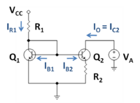
Widlar current source using bipolar transistors
(CC) Image: John R. Brews
Widlar current source using bipolar transistors
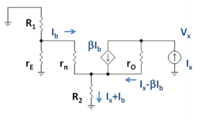
Small-signal circuit for finding output resistance of the Widlar source
(CC) Image: John R. Brews
Small-signal circuit for finding output resistance of the Widlar source
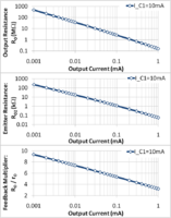
Design trade-off between output resistance and output current in Widlar source
(CC) Image: John R. Brews
Design trade-off between output resistance and output current in Widlar source
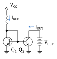
A current mirror implemented with npn bipolar transistors using a resistor to set the reference current IREF; VCC = supply voltage.
(PD) Image: John R. Brews
A current mirror implemented with npn bipolar transistors using a resistor to set the reference current IREF; VCC = supply voltage.
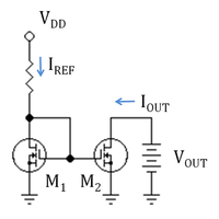
An n-channel MOSFET current mirror with a resistor to set the reference current
(PD) Image: John R. Brews
An n-channel MOSFET current mirror with a resistor to set the reference current
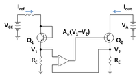
Gain-boosted current mirror with op amp feedback to increase output resistance.
(PD) Image: John R. Brews
Gain-boosted current mirror with op amp feedback to increase output resistance.
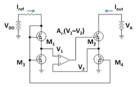
MOSFET version of wide-swing current mirror; M1 and M2 are in active mode
(PD) Image: John R. Brews
MOSFET version of wide-swing current mirror; M1 and M2 are in active mode
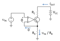
Operational-amplifier based current sink. Because the op amp is modeled as a nullor, op amp input variables are zero regardless of the values for its output variables.
(PD) Image: John R. Brews
Operational-amplifier based current sink. Because the op amp is modeled as a nullor, op amp input variables are zero regardless of the values for its output variables.
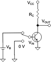
A digital inverter circuit using a bipolar transistor.
(PD) Image: John R. Brews
A digital inverter circuit using a bipolar transistor.
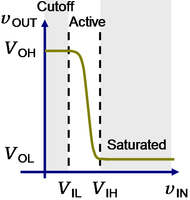
Transfer characteristic of bipolar inverter showing modes.
(PD) Image: John R. Brews
Transfer characteristic of bipolar inverter showing modes.
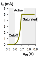
Collector current vs. input voltage for a bipolar inverter with VCC=5V and RC=1kΩ.
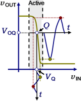
Input and output signals for bipolar inverter used as an amplifier.
(PD) Image: John R. Brews
Input and output signals for bipolar inverter used as an amplifier.
Two-port network with symbol definitions.
(PD) Image: John R. Brews
Two-port network with symbol definitions.
Z-equivalent two port showing independent variables I1 and I2.
(PD) Image: John R. Brews
Z-equivalent two port showing independent variables I1 and I2.
Y-equivalent two port showing independent variables
(PD) Image: John R. Brews
Y-equivalent two port showing independent variables
H-equivalent two-port showing independent variables
(PD) Image: John R. Brews
H-equivalent two-port showing independent variables
G-equivalent two-port showing independent variables
(PD) Image: John R. Brews
G-equivalent two-port showing independent variables
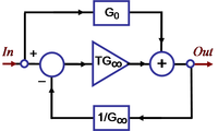
Block diagram for asymptotic gain model
(PD) Image: John R. Brews
Block diagram for asymptotic gain model
Possible signal-flow graph for the asymptotic gain model
(PD) Image: John R. Brews
Possible signal-flow graph for the asymptotic gain model
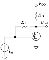
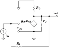
MOSFET transresistance feedback amplifier.
(PD) Image: John R. Brews
MOSFET transresistance feedback amplifier.
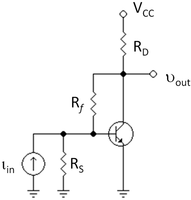
Collector-to-base biased bipolar amplifier.
(PD) Image: John R. Brews
Collector-to-base biased bipolar amplifier.
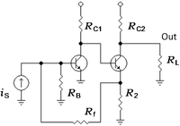
Two-transistor feedback amplifier; any source impedance RS is lumped in with the base resistor RB.
(PD) Image: John R. Brews
Two-transistor feedback amplifier; any source impedance RS is lumped in with the base resistor RB.

Small-signal circuits

Small-signal circuits
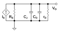
Small-signal circuit for pn-diode driven by a current signal represented as a Norton source.
(PD) Image: John R. Brews
Small-signal circuit for pn-diode driven by a current signal represented as a Norton source.
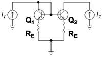
Bipolar current mirror with emitter resistors
(PD) Image: John R. Brews
Bipolar current mirror with emitter resistors
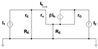
Small-signal circuit for bipolar current mirror
(PD) Image: John R. Brews
Small-signal circuit for bipolar current mirror
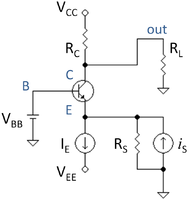
Common base circuit with active load and current drive.
(PD) Image: John R. Brews
Common base circuit with active load and current drive.
Common-base amplifier with AC current source I1 as signal input
(PD) Image: John R. Brews
Common-base amplifier with AC current source I1 as signal input
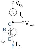
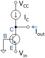
Bipolar transistor with base grounded and signal applied to emitter.
(PD) Image: John R. Brews
Bipolar transistor with base grounded and signal applied to emitter.
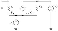
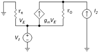
Common-base amplifier with AC voltage source V1 as signal input
(PD) Image: John R. Brews
Common-base amplifier with AC voltage source V1 as signal input
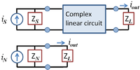
The result of applying Norton's theorem.
(PD) Image: John R. Brews
The result of applying Norton's theorem.
Bipolar current buffer.
(PD) Image: John R. Brews
Bipolar current buffer.
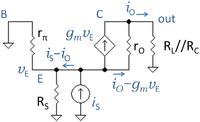
Small-signal circuit to find output current.
(PD) Image: John R. Brews
Small-signal circuit to find output current.
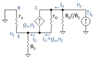
Small-signal circuit with test current iX to find Norton resistance.
(PD) Image: John R. Brews
Small-signal circuit with test current iX to find Norton resistance.
The result of applying Thévenin's theorem.
(PD) Image: John R. Brews
The result of applying Thévenin's theorem.
Bipolar buffer.
(PD) Image: John R. Brews
Bipolar buffer.
Small-signal circuit for voltage follower.
(PD) Image: John R, Brews
Small-signal circuit for voltage follower.
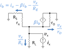
Determination of the small-signal output resistance.
(PD) Image: John R. Brews
Determination of the small-signal output resistance.
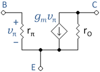
Simplified, low-frequency hybrid-pi BJT model.
(PD) Image: John R. Brews
Simplified, low-frequency hybrid-pi BJT model.
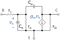
Bipolar hybrid-pi model with parasitic capacitances.
(PD) Image: John R. Brews
Bipolar hybrid-pi model with parasitic capacitances.
Simplified, low-frequency hybrid-pi BJT model.
(PD) Image: John R. Brews
Simplified, low-frequency hybrid-pi BJT model.
Bipolar hybrid-pi model with parasitic capacitances.
(PD) Image: John R. Brews
Bipolar hybrid-pi model with parasitic capacitances.
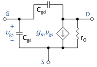
Simplified, three-terminal MOSFET hybrid-pi model.
(PD) Image: John R. Brews
Simplified, three-terminal MOSFET hybrid-pi model.
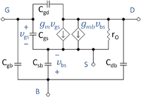
Four-terminal small-signal MOSFET circuit.
(PD) Image: John R. Brews
Four-terminal small-signal MOSFET circuit.
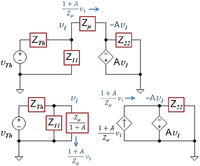
Miller effect: These two circuits are equivalent.
(PD) Image: John R. Brews
Miller effect: These two circuits are equivalent.
Small-signal circuit for transresistance amplifier
(PD) Image: John R. Brews
Small-signal circuit for transresistance amplifier
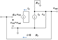
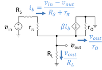
Small-signal circuit with return path broken and test current it driving amplifier at the break.
(PD) Image: John R. Brews
Small-signal circuit with return path broken and test current it driving amplifier at the break.
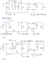
Three small-signal schematics used to discuss the asymptotic gain model
(PD) Image: John R. Brews
Three small-signal schematics used to discuss the asymptotic gain model

Return ratio

Return ratio
Left - small-signal circuit corresponding to bipolar amplifier; Center - inserting independent source and marking leads to be cut; Right - cutting the dependent source free and short-circuiting broken leads.
(PD) Image: John R. Brews
Left - small-signal circuit corresponding to bipolar amplifier; Center - inserting independent source and marking leads to be cut; Right - cutting the dependent source free and short-circuiting broken leads.

Amplifiers

Amplifiers
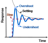
Some terms used to describe step response in time domain.
(PD) Image: John R. Brews
Some terms used to describe step response in time domain.
Ideal negative feedback model; open loop gain is AOL and feedback factor is β.
(PD) Image: John R. Brews
Ideal negative feedback model; open loop gain is AOL and feedback factor is β.
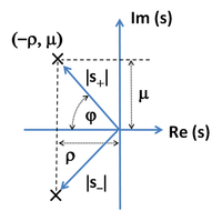
Conjugate pole locations for step response of two-pole feedback amplifier.
(PD) Image: John R. Brews
Conjugate pole locations for step response of two-pole feedback amplifier.
Step-response of a linear two-pole feedback amplifier.
(PD) Image: John R. Brews
Step-response of a linear two-pole feedback amplifier.
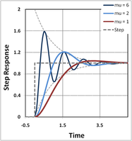
Step response for three values of time constant ratio.
(PD) Image: John R. Brews
Step response for three values of time constant ratio.
Bode gain plot to find phase margin of two-pole amplifier.
(PD) Image: John R. Brews
Bode gain plot to find phase margin of two-pole amplifier.
The Bode plot for a first-order (one-pole) highpass filter
(PD) Image: John R. Brews
The Bode plot for a first-order (one-pole) highpass filter
The Bode plot for a first-order (one-pole) lowpass filter
(PD) Image: John R. Brews
The Bode plot for a first-order (one-pole) lowpass filter
Bode magnitude plot for zero and for low-pass pole
(PD) Image: John R. Brews
Bode magnitude plot for zero and for low-pass pole
Bode phase plot for zero and for low-pass pole
(PD) Image: John R. Brews
Bode phase plot for zero and for low-pass pole
Bode magnitude plot for pole-zero combination; the location of the zero is ten times higher than in above figures
(PD) Image: John R. Brews
Bode magnitude plot for pole-zero combination; the location of the zero is ten times higher than in above figures
Bode phase plot for pole-zero combination; the location of the zero is ten times higher than in above figures
(PD) Image: John R. Brews
Bode phase plot for pole-zero combination; the location of the zero is ten times higher than in above figures
Gain of feedback amplifier AFB in dB and corresponding open-loop amplifier AOL.
(PD) Image: John R. Brews
Gain of feedback amplifier AFB in dB and corresponding open-loop amplifier AOL.
Phase of feedback amplifier °AFB in degrees and corresponding open-loop amplifier °AOL.
(PD) Image: John R. Brews
Phase of feedback amplifier °AFB in degrees and corresponding open-loop amplifier °AOL.
Gain of feedback amplifier AFB in dB and corresponding open-loop amplifier AOL.
(PD) Image: John R. Brews
Gain of feedback amplifier AFB in dB and corresponding open-loop amplifier AOL.
Phase of feedback amplifier AFB in degrees and corresponding open-loop amplifier AOL.
(PD) Image: John R. Brews
Phase of feedback amplifier AFB in degrees and corresponding open-loop amplifier AOL.
Operational amplifier with compensation capacitor CC between input and output to cause pole splitting.
(PD) Image: John R. Brews
Operational amplifier with compensation capacitor CC between input and output to cause pole splitting.
Operational amplifier with compensation capacitor transformed using Miller's theorem to replace the compensation capacitor with a Miller capacitor at the input and a frequency-dependent current source at the output.
(PD) Image: John R. Brews
Operational amplifier with compensation capacitor transformed using Miller's theorem to replace the compensation capacitor with a Miller capacitor at the input and a frequency-dependent current source at the output.
Idealized Bode plot for a two pole amplifier design.
(PD) Image: John R. Brews
Idealized Bode plot for a two pole amplifier design.
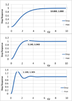
Miller capacitance at low frequencies CM (top) and compensation capacitor CC (bottom) as a function of gain
(PD) Image: John R. Brews
Miller capacitance at low frequencies CM (top) and compensation capacitor CC (bottom) as a function of gain